Difference between revisions of "PCB milling machine"
| Line 247: | Line 247: | ||
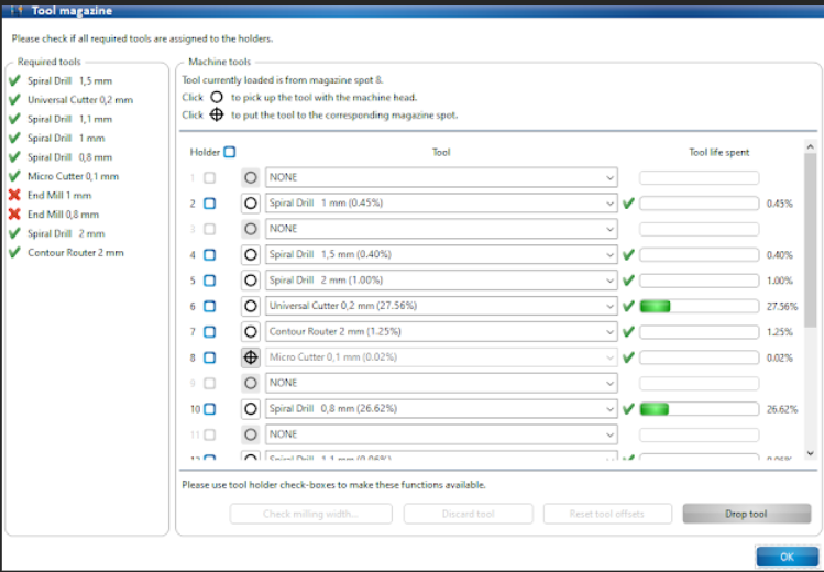
| − | 19. If there are tools that are missing, '''Click''' on [Edit] → [Tool magazine…] The tools required for circuit board production are displayed. Tools that are missing in the tool magazine are marked with a red X. [[File: Tool magazine display.png|border|center| | + | 19. If there are tools that are missing, '''Click''' on [Edit] → [Tool magazine…] The tools required for circuit board production are displayed. Tools that are missing in the tool magazine are marked with a red X. [[File: Tool magazine display.png|border|center|550x800px| Tool magazine display|link=Special:FilePath/Tool_magazine_display.png]] |
<div class="center" style="width: auto; margin-left: auto; margin-right: auto;">Figure 24. Tool magazine display </div> | <div class="center" style="width: auto; margin-left: auto; margin-right: auto;">Figure 24. Tool magazine display </div> | ||
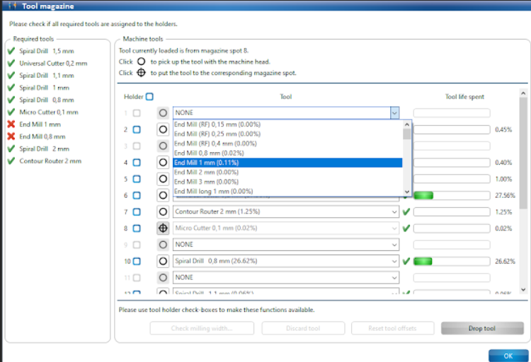
| − | 20. In the tool magazine, '''assign''' the required tools to the tool holder positions:[[File:Assigning tools in the correct tool holder position .png|border|center| | + | 20. In the tool magazine, '''assign''' the required tools to the tool holder positions:[[File:Assigning tools in the correct tool holder position .png|border|center|550x800px|Assigning tools in the correct tool holder position|link=Special:FilePath/Assigning_tools_in_the_correct_tool_holder_position_.png]] |
<div class="center" style="width: auto; margin-left: auto; margin-right: auto;">Figure 25. Assigning tools in the correct tool holder position</div> | <div class="center" style="width: auto; margin-left: auto; margin-right: auto;">Figure 25. Assigning tools in the correct tool holder position</div> | ||
Revision as of 19:28, 21 June 2024
This document will go through an overview of a PCB mill machine including important information on operating the system and the associated software programs and will also describe a typical production process.
Background
A Printed Circuit Board (PCB) is a board that has pads that are connected with traces (lines) which make a circuit. It allows electrical components to be connected and get power when they are soldered to this board.
Solder is metal that glues the component to the board and it provides the connection between them.
A PCB is made up of many layers of different materials, as shown in Figure 1.

- Substrate (FR4): The substrate (FR4) is fiberglass which gives the board rigidity and insulates each side from the other.
- Copper: The copper is the conductive material in the board. It can be only on one side of the board or more commonly on both sides to have a double-sided board.
- Soldermask:The next layer, the soldermask, is placed on top of the copper to avoid unwanted contact from other conductive elements.
- Silkscreen:The white silkscreen is then placed on top to indicate the position of different components or any notations you would like to add.
Figure 1 shows a 2-layer board, but more inner layers can be created by sandwiching multiple 2-layer substrates. If connections need to be made between layers, then holes need to be drilled then plated through inside with metal to make the connection between the layers (Figure 2). These holes are called vias. We are making a 2-layer through hole board, which means our components will have pins that pass through the PCB and will be soldered on the opposite side.
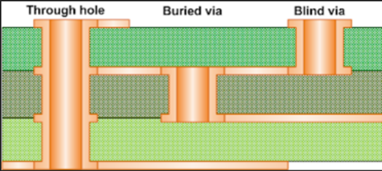
Through hole vias are the most common and the cheapest, since it is easiest to drill a hole all the way through a piece of material with layers that have already been sandwiched together.
Safety
This section provides an overview of all important safety aspects for protecting persons as well as for a safe and fault-free operation of the system.
The system has been developed especially for micro material processing and approved for the following processing procedures and materials:
- Processing procedures
- Processing of single-sided and double-sided base material
- Processing of multi-layer material
- Processing of SMD solder paste stencils
- Processing of solder stop films
- Engraving of signs or housing panels (e.g., front or rear plates)
- Drilling of plane materials using drilling tools
Materials
- GFRP or CFRP base material
- PTFE or ceramic-filled base material
- non-ferrous metals like
- aluminum acc. to DIN EN 573:EN AW-6012
- brass acc. to DIN EN 1412:CW603N
- polyoxymethylene
- ABS copolymers
- Necuron ®
Safety rules
- Never grasp moving components when the system is operating.
- Observe the follow-up time of the spindle. Before doing any work in the processing area or on the processing head, ensure that no component is still moving.
- Before switching on the system, always ensure that no items and no parts are in the processing area.
- The collet always has to be equipped with a tool even when the system is not in use (standby, switched off, transport, storage). Ensure that a tool is in the collet, or a tool is in the tool magazine where it can be picked up by the collet.
- Only work with an extraction system that is switched on and is working properly.
- Always use the delivered insertion tool.
- Always store the tools in the toolbox.
- Never touch the processing head during operation.
- Defective components that are under pressure when operating the system must be replaced immediately by sufficiently qualified personnel.
- Ensure that the extraction system is switched on and is working properly.
Using the PCB milling machine
Switching ON the system
1.Turn on the machine by pressing the on/off switch at the back.

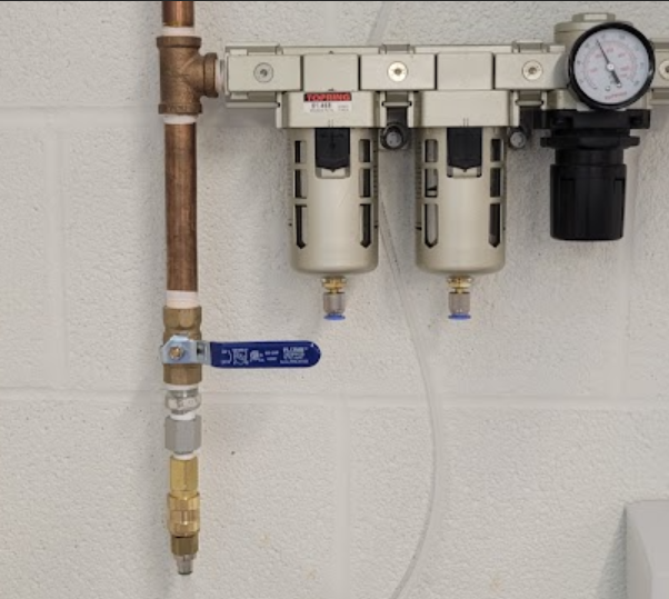
2.Turn on the compressor by turning the blue valve on the wall near the sink.
3.Start the LPFK software by clicking on the desktop shortcut or on [Start] → (All) [Programs] → [LPKF Laser & Electronics] → [CircuitPro PM].
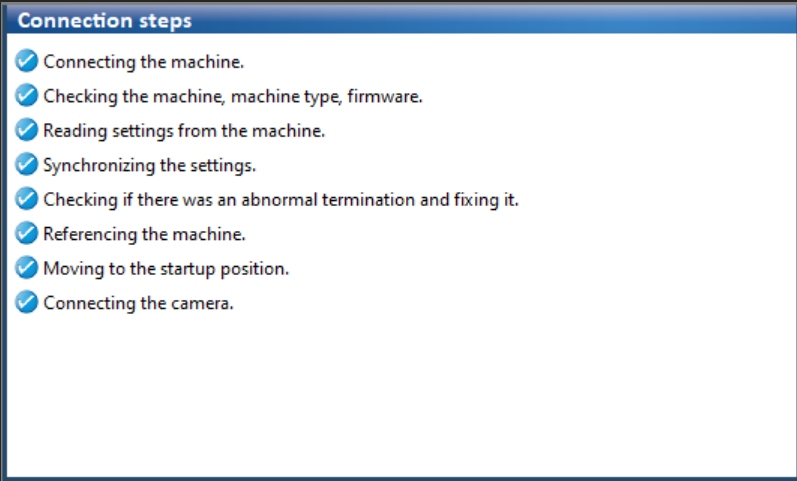
The machine will automatically be initialized, and the following dialog will be displayed.
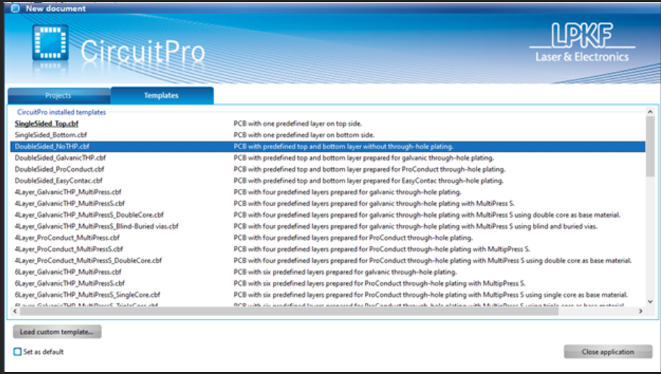
4.In the dialog that is displayed, you can select the template of your choice. For now, select the template DoubleSided_NoTHP.cbf in the tab Templates to create a double-sided PCB.
The dialog will close, and the user interface will change as follows:
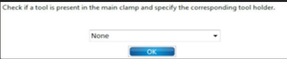
5.Whenever the machine or the software has not been shut down properly. The last tool status is unknown. If that happens, you will be prompted to put down the tool possibly being in the collet into the corresponding tool holder.
Preparing the data
1. At this point, you should have a file that was given to you at the beginning of this workshop. Download that file and save it on your computer.
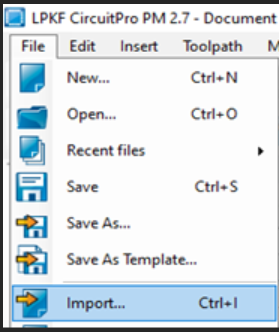
2. Click on [File] → [Import].
3. You will be prompted to open the files of your PCB. Navigate to the folder that contains the greber files (.gbr), select all the files and click on [Open].
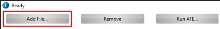
4. Click on [Add file...] on the bottom left to navigate to the folder that contains the drill files and add all the files.
5. Assign the imported files to the corresponding layers:
| File name | Layer/Template |
|---|---|
| copper_bottom.gbr | BottomLayer |
| copper_top.gbr | TopLayer |
| profile.gbr | BoardOutline |
| silkscreen_bottom.gbr | BottomLayer |
| silkscreen_top.gbr | TopLayer |
| drill_1_16.xln | DrillUnplated |
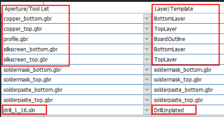
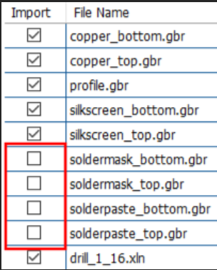
6. Uncheck the rest of the files that are unused
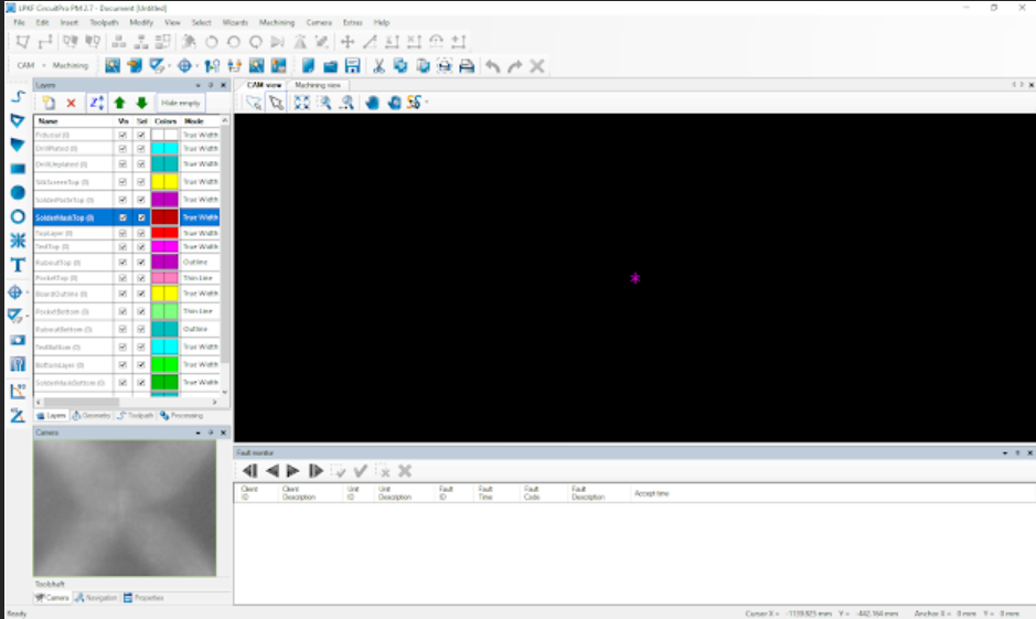
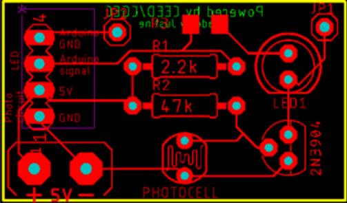
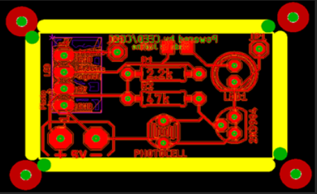
7. Click on [Ok]. The PCB design should appear on the screen.
8. Next, draw the rubout area of the design. Click on [Insert] → [Rubout area] → [RuboutTop].
9. Draw a rectangle on all the places you would like to have rub outs, as shown in the following figure (purple rectangle). First left click and release the mouse, then move the mouse to place the rectangle and left click again to confirm.
10. Click on [Close].
11. Now let create fiducials. Click on [Insert] → [Fiducials] → [Fiducial…]
12. In the CAM view click on the positions where you want to place the fiducials (four red circles around the yellow square).
13. Click on [close].
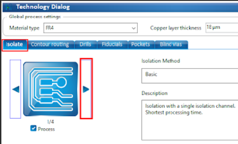
14.To generate the toolpath, click on [Toolpath] → [Technology dialog…]
The following dialog will display.
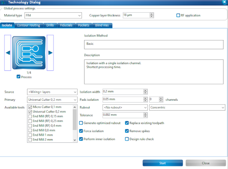
15. Click on the right arrow button in the group Isolate until the Isolation Method Partial rubout is displayed.
16. Deactivate the function Pockets by clicking on the corresponding check mark.
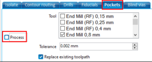
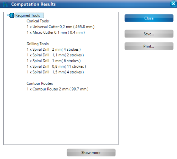
17. Click on [Start]. The computation results and the tools required for the project are displayed. Check whether all required tools are available and placed in the machine. Steps to take if tools are missing are available below.
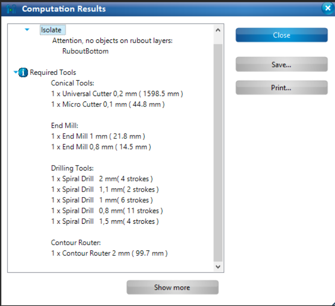
18. Click on [Close]. The dialog with the computation results is closed and the CAM view changes as the following figure. The toolpaths have been generated.
19. If there are tools that are missing, Click on [Edit] → [Tool magazine…] The tools required for circuit board production are displayed. Tools that are missing in the tool magazine are marked with a red X.
20. In the tool magazine, assign the required tools to the tool holder positions:
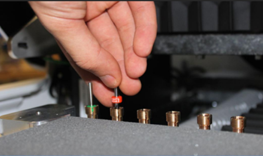
21. Once all tools have been assigned successfully, Open the machine cover, and insert the tools into the tool holders of the tool magazine. Ensure that the tools are inserted into the tool holder positions that you have assigned in the dialog Tool magazine!
22. Click on [OK].
Processing the material
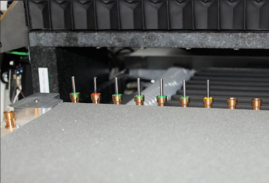
- Ensure that the processing table is clean (No debris).
- Place the supplied sinter plate onto the processing table (White rectangle)
- Place the underlay material (2) onto the sinter plate (1)
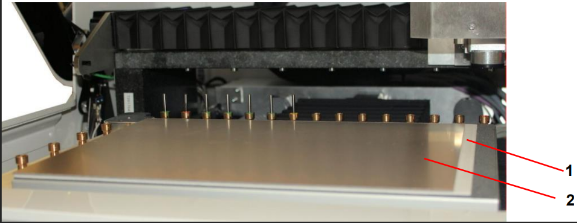
- Put some tape to immobilize the material to be processed along its edges onto the processing table
Figure 29. Material fastened
- Click on [Machining] → [Process all]. Ensure that the value <Process all> is selected in the group Operate so that all phases are processed.
Figure 30. Operate menu
- Click on .
- Mount the material onto the processing table if not already done. Click on [OK].
- Enter the correct values for the material used in the dialog Material settings. In the group Application, the material PCB is selected as default. Edit the values for the copper layer thickness and material thickness if necessary (shouldn`t be the case for this operation).
- For defining the material area, move the dialog Material settings to the side. In the Machining view click on the position of the screen that represents the right rear corner of your material
Figure 31. Defining the material area (right corner)
- The processing head moves to the right rear corner. Click on [P2] in the dialog Material settings.
- Click on the position of the screen that represents the front left corner of your material
Figure 32. Defining the material area (left corner)
- The processing head moves to the front left corner. Click on [P1] in the dialog Material settings.
- Click on [OK].
- Using your mouse, move the toolpaths in the machining view and place it around the top left corner of your material.
- Click on [Continue].
- The work has started. If the spindle motor has not run yet, a 2-minute warm-up phase is started.
- If you are asked to define the machine area for milling-width checking (Figure 33), with the mouse click on an area in your material that will not affect your design (Figure 34) and click on [OK]. The machine will trace a line (Figure 35) and use the camera to measure the milling width area.
Figure 33. Popup display for definition of machine area
Figure 34. Defining the machine area (define position)
- A line will be trace at that location
Figure 35. Defining the machine area (line tracing)
- In the pop-up screen, Accept the focusing height.
- Click on [Store correction].
Figure 36. Store correction menu
- When it’s time to flip the material, remove the adhesive tape, lift the material, turn the material over along the vertical axis, fix it with adhesive tape again.
- Click on [OK]. The machining view changes. The orientation of the layout is adapted to the orientation of the material. The side of the material to be processed is now the top side.
- When the work is done, remove your cut PCB.